AN217
Rev. 0.2 5
2.2.3. Offset DAC
The ADC features an internal dedicated DAC that is used to adjust the measurement offset of the ADC. This can
be used as a software controlled tare function in the end-product. For example, the offset DAC could be used to
remove the platform weight in a weigh scale application in order to measure only the scale contents of interest. The
offset DAC can make a signed adjustment to approximately ±1/2 of the ADC’s input range with any PGA gain
setting. See the “Offset DAC” section of the ADC0 chapter of the data sheet for complete information on how to
configure the offset DAC.
Note: Small external system and ADC offset errors are corrected via the ADC’s built-in calibration function. The offset DAC is
used to zero or tare a measurement as a function of the end-product and is not intended for calibration.
2.2.4. Input Buffers
Two input buffers can be used to provide a high-impedance input to the ADC when a high-impedance sensor is
measured (i.e., the sensor will source very little current). One input buffer is used to measure signals with voltages
in the upper half of the voltage supply range (“high” input buffer) and one is used for the lower half of the voltage
supply range (“low” input buffer).
While the on-chip input buffers are adequate for many applications, they may not be sufficient for highly sensitive
measurements at the highest resolution (i.e, 24-bits). This is because they introduce 1/f noise, which will appear as
voltage “drift” in the measurement. For this reason, the input buffers can be bypassed, and an external buffer or
amplifier can be used. The input buffers are software controlled; therefore, they can easily be evaluated. See the
“Input Buffers” section of the ADC0 chapter of the data sheet for complete information and specifications for the
input buffers.
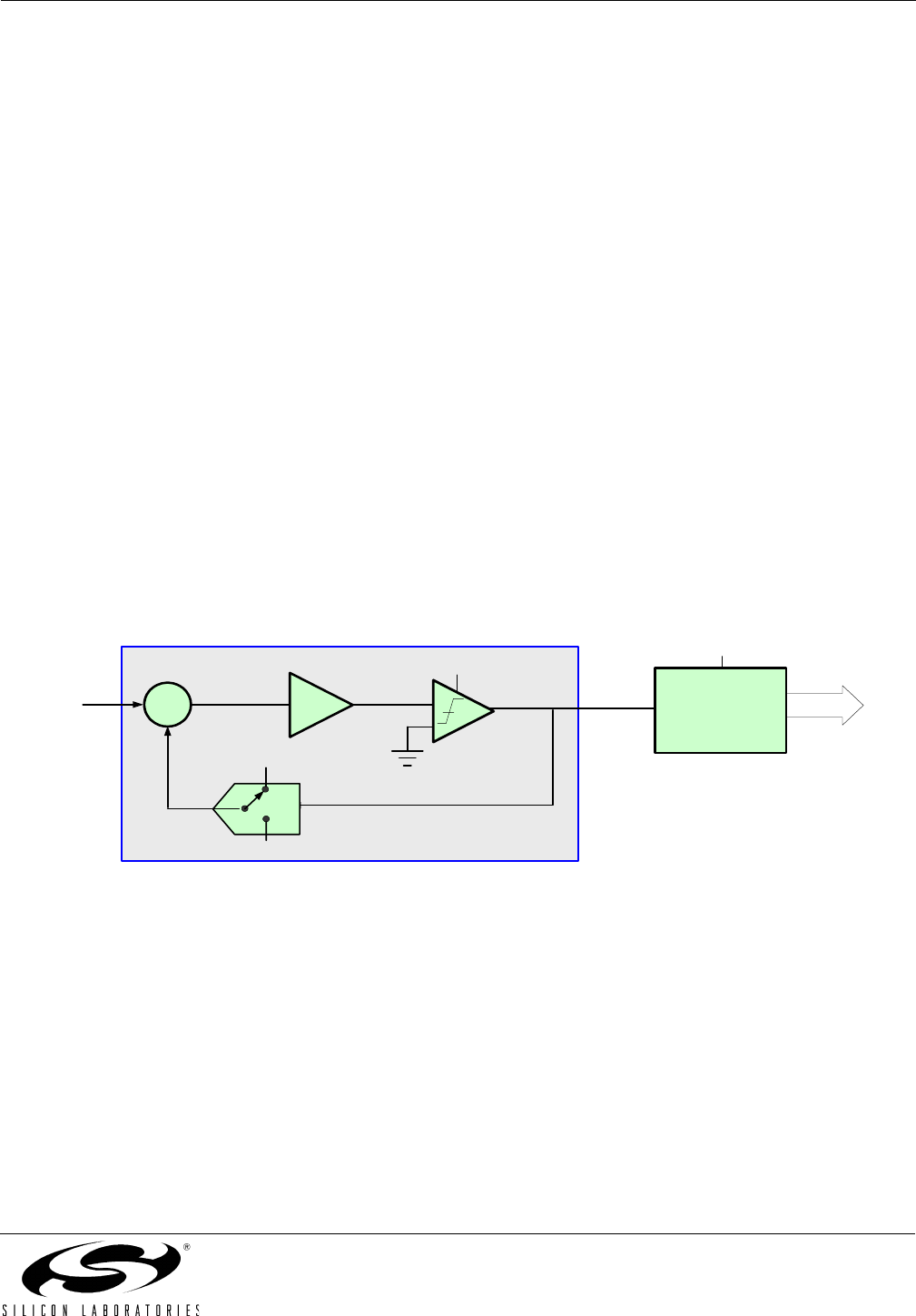
2.2.5. The Modulator
The modulator’s function is to oversample the measured signal, shape the noise such that it is reduced in the
signal bandwidth, and produce a series of 1-bit output codes. These output codes will have a density and order of
1s and 0s that are used to produce a high-resolution digital representation of the input signal (the modulator output
is digitally filtered to obtain large output words).
Figure 3. Modulator and Digital Filter
In order to oversample the input signal and still obtain a reasonable output word rate, the modulator is configured
to operate at a high frequency. The modulator is designed with an integrator in a feedback loop. This integrator
shapes the noise so that the digital filter removes the maximum amount of the noise. This is the advantage of the
delta-sigma converter. To get this performance, it is important to configure the modulator to operate at its specified
frequency. For the C8051F35x ADC, the modulator frequency should be 2.4576 MHz for optimum
performance.
The modulator clock (MDCLK) is derived from the MCU system clock. To allow flexibility in the use of many system
clock sources, the user has access to the divider in the ADC0 Modulator Clock Divisor (ADC0CLK) register (see
SFR Definition 2.2). The MDCLK value is set using the ADC0CLK register (see SFR Definition 2.2) to achieve a
frequency of 2.4576 MHz according to Equation 1:
Equation 1. Configure Modulator Clock Frequency
MODULATOR
∑
INTEGRATOR
LATCHED
COMPARATOR
(1-BIT ADC)
BIT
STREAM
Analog
Input
CLOCK (Kfs)
1-BIT
DAC
DATA
+
-
∫
+VREF
-VREF
CLOCK (fs)
DIGITAL
FILTER
MDCLK SYSCLK()ADC0CLK 1+()⁄=
 Manymanuals.com
 Manymanuals.de
 Manymanuals.fr
 Manymanuals.it
 Manymanuals.pl
 Manymanuals.cz
 Manymanuals.es
 Manymanuals-pt.com
Comments to this Manuals