ADC12EU050
SNAS444I –JANUARY 2008–REVISED APRIL 2013
www.ti.com
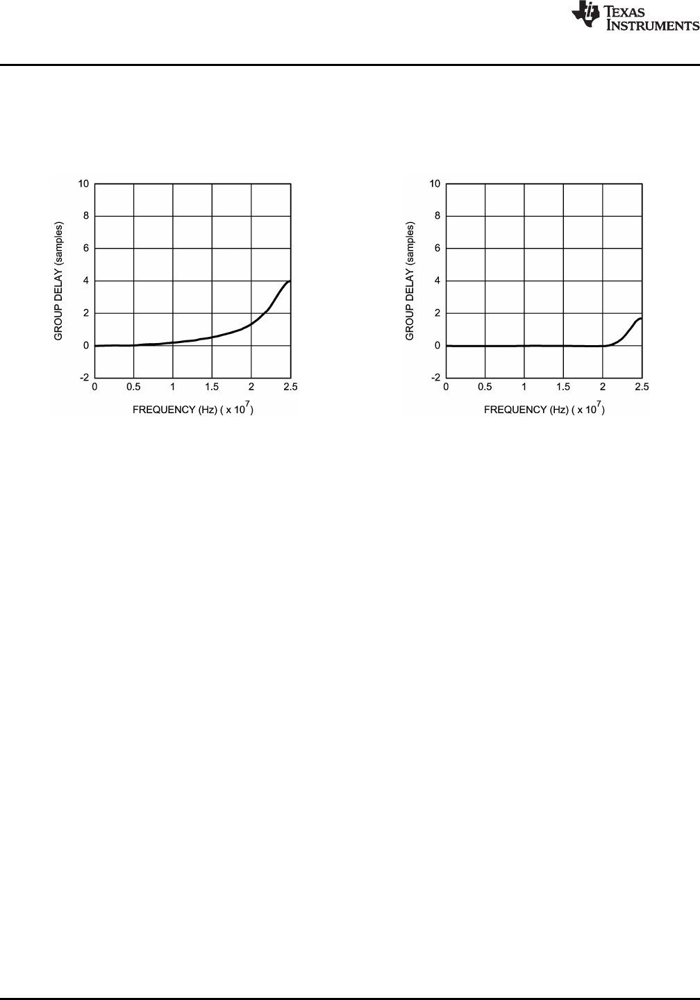
Such steep digital filters introduce group delay problems, but the ADC12EU050 includes a digital equalizer,
which reduces group delay ripple variation to less than 0.05 samples. In applications where group delay is not of
concern, the equalizer can be turned off through the SPI interface in order to save power.
The following two diagrams show the group delay ripple of the digital decimation filter at 50MSPS, firstly with the
equalizer disabled, and secondly with the equalizer enabled.
Figure 10. Group Delay with Equalizer Off Figure 11. Group Delay with Equalizer On
SERIAL DATA OUTPUTS
Sampled data is transformed into high speed serial LVDS/SLVS output data streams. The low amplitude
differential signal swings of LVDS/SLVS help to reduce digital system noise.
It is possible to select between LVDS and SLVS modes by simple programming through the SPI control
interface. The output common mode can also be programmed through the SPI control interface, allowing it to be
adjusted based on the value of V
DR
.
POWER MANAGEMENT MODES
The ADC12EU050 operates normally at ultra-low power levels. In addition, several power management modes
are provided:
• Power Down (accessible through PD bit of Top Control Register)
• Sleep (SLEEP pin, or SLEEP bit of Top Control Register)
• Single channel power down (PD0-7 of ADC/LVDS Channel Power Down Register)
Power Down is the lowest power consumption mode, but with a longer wake-up time than Sleep mode. In power
down mode, all circuits in the chip are turned off, including the PLL, reference and bias circuits.
Power consumption in Sleep mode is higher than in Power Down mode, but pin access (SLEEP pin) and fast
wake-up enables duty cycle powering of the ADC.
The device also allows channel by channel power-down through the ADC/LVDS Channel Power Down register.
When a single channel is powered down, the sigma delta modulator, digital decimating filter and LVDS outputs
for that channel will be shut off, with the corresponding single channel reduction in power consumption.
SPI CONTROL INTERFACE
The ADC12EU050 provides configurability via the serial control interface. This provides IOR mode control power
management control, output configuration control, data output test patterns to provide LVDS/SLVS training
sequences, as well as many other user configurable options. Full details of the SPI registers can be found in
Programming Guide.
The SPI pins (S
DATA
, S
CLK
, S
SEL
), as well as the pins RST and SLEEP, have been designed to operate with
voltage levels up to 2.5V, despite the low 1.2V core voltage. As a result, no external level shift components are
required for this control interface.
16 Submit Documentation Feedback Copyright © 2008–2013, Texas Instruments Incorporated
Product Folder Links: ADC12EU050
 (34 pages)
 (28 pages)
 Manymanuals.com
 Manymanuals.de
 Manymanuals.fr
 Manymanuals.it
 Manymanuals.pl
 Manymanuals.cz
 Manymanuals.es
 Manymanuals-pt.com
Comments to this Manuals