D
CAP
DAC
Bias
DAC
R
DCAP
C
DCAP
1.5 k5
ADC12EU050 ä? Modulator
AGND
ADC12EU050
www.ti.com
SNAS444I –JANUARY 2008–REVISED APRIL 2013
D
CAP
CAPACITOR SELECTION
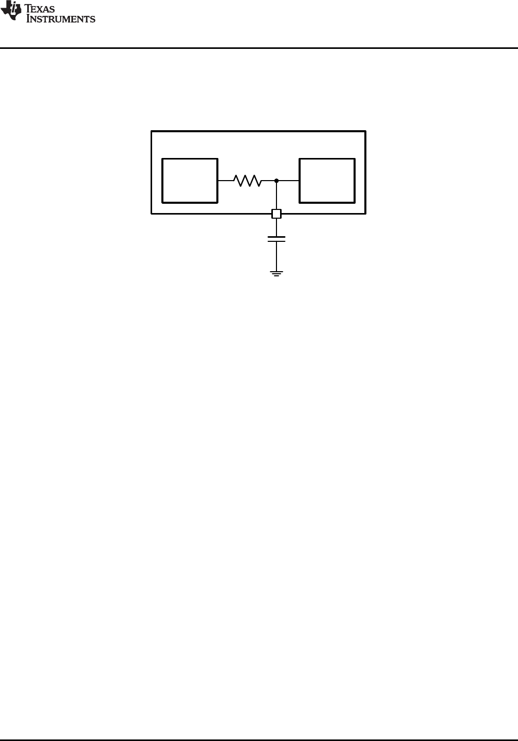
The D
CAP
pin provides the capacitance for the low pass filter between the DAC bias block and the DAC in the
sigma-delta modulator. The filter blocks noise from the DAC Bias block from entering the DAC. Any noise which
passes through this filter will be seen in the spectrum as side skirts around the carrier. The filter circuit, which is
a first order RC filter, is shown in the diagram below.
Figure 23. D
CAP
RC Filter
The D
CAP
pin must be connected to AGND through a low leakage, minimum 100nF capacitor. If the application is
especially sensitive to close to the carrier phase noise, then it is recommended to increase D
CAP
, up to a
maximum of 10µF. For other applications where close to the carrier phase noise is not important, the capacitor
can be kept small in order to reduce costs and minimise board space. The corner frequency of this filter is
determined by the equation:
f = 1/(2πR
DCAP
C
DCAP
) (2)
BOARD LAYOUT CONSIDERATIONS
Proper grounding, layout and routing are essential to ensure accurate conversion in any high speed ADC.
Maintaining separate analog and digital areas of the board is recommended in order to achieve the specified
performance. This includes using a split ground plane, since the significant digital portion of the chip can produce
noise on the digital/IO ground (DGND).
When designing the ADC12EU050 into a system, It is critical that the exposed pad is connected to analog
ground (AGND). The exposed pad provides the analog ground connection for the ADC12EU050, and so this
connection is required for electrical rather than thermal reasons.
It is recommended to decouple the power supplies using a large capacitor (e.g. 47µF) for low frequency noise,
and small capacitors (e.g. 100nF) placed close to each supply pin.
Analog and digital supplies (V
A
and V
D
) may be provided from the same supply, however in this case it is
recommended that the supplies are isolated from each other with a ferrite bead or inductor. If the IO driver supply
(V
DR
) is 1.2V, then it may also be taken from the same supply, with isolation as described above.
The clock and data output traces, as well as the clock input trace (when using a differential input clock), should
be routed as 100Ω impedance differential pairs. If not using the option for 100Ω internal termination, then the
clock and data output trances should be terminated with a 100Ω resistor close to the receiver.
If the system requires regulators to provide the ADC12EU050 1.2V operating voltage, Texas Instruments
recommends the LP3878SD-ADJ Low Noise “Ceramic Stable” Adjustable Regulator or the LP3879 Low Noise
“Ceramic Stable” Regulator. Datasheets for both parts are available from the Texas Instruments website.
Copyright © 2008–2013, Texas Instruments Incorporated Submit Documentation Feedback 25
Product Folder Links: ADC12EU050
 (34 pages)
 (28 pages)
 Manymanuals.com
 Manymanuals.de
 Manymanuals.fr
 Manymanuals.it
 Manymanuals.pl
 Manymanuals.cz
 Manymanuals.es
 Manymanuals-pt.com
Comments to this Manuals