ADC12EU050
www.ti.com
SNAS444I –JANUARY 2008–REVISED APRIL 2013
ELECTRICAL CHARACTERISTICS (continued)
Unless otherwise specified, the following conditions apply: V
A
= V
D
= 1.2V; V
DR
= 1.2V; V
REF
= internal; R
REF
= 10kohm ±1%;
C
L
= 5pF; 100Ω terminated at the receiver; f
CLK
= 45MHz; f
S
= 45MSPS. Boldface limits apply for T
A
= T
MIN
to T
MAX
; All other
limits apply for T
A
= +25°C.
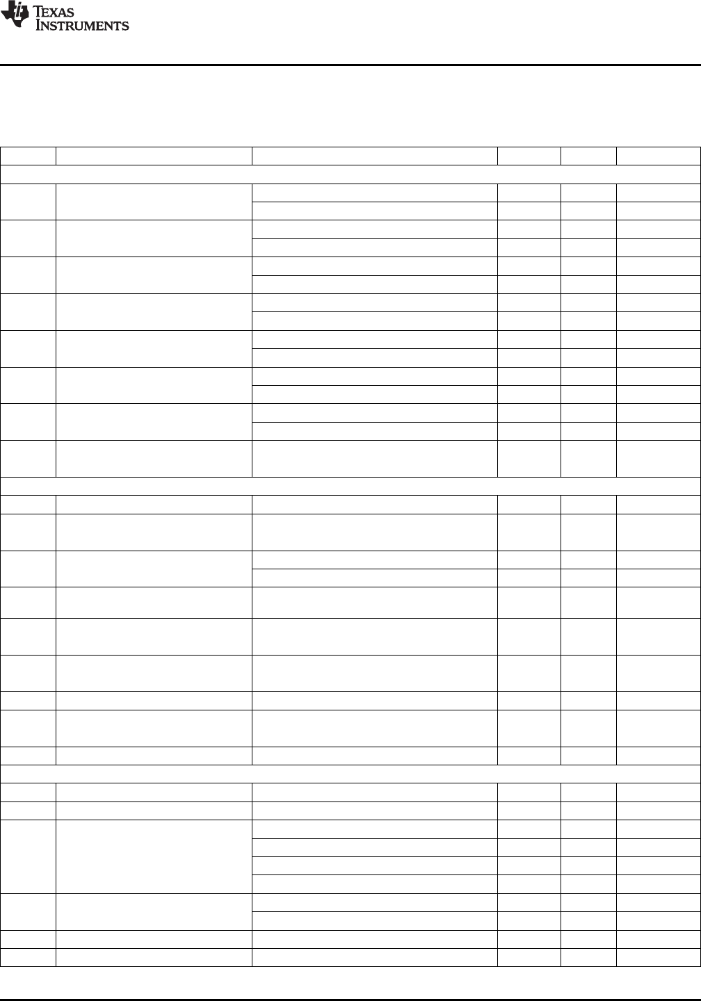
Symbol Parameter Conditions Typical
(1)
Limits Units
Dynamic Converter Characteristics – Instant Overload Recovery (IOR) On
f
CLK
= 45MHz, f
IN
= 4.4MHz, V
IN
= -0.5dBFS 67.6 65.5 dBFS (min)
SNR Signal-to-Noise Ratio
(3)
f
CLK
= 45MHz, f
IN
= 9.5MHz, V
IN
= -0.5dBFS 67.4 dBFS
f
CLK
= 45MHz, f
IN
= 4.4MHz, V
IN
= -0.5dBFS 67.0 61.5 dBFS (min)
SINAD Signal-to-Noise and Distortion
(3)
f
CLK
= 45MHz, f
IN
= 9.5MHz, V
IN
= -0.5dBFS 67.0 dBFS
f
CLK
= 45MHz, f
IN
= 4.4MHz, V
IN
= -0.5dBFS 10.8 9.9 Bits (min)
ENOB Effective Number of Bits
f
CLK
= 45MHz, f
IN
= 9.5MHz, V
IN
= -0.5dBFS 10.8 Bits
f
CLK
= 45MHz, f
IN
= 4.4MHz, V
IN
= -0.5dBFS -76 -64 dBc (max)
THD Total Harmonic Disortion
f
CLK
= 45MHz, f
IN
= 9.5MHz, V
IN
= -0.5dBFS -77 dBc
f
CLK
= 45MHz, f
IN
= 4.4MHz, V
IN
= -0.5dBFS -80 -65 dBc (max)
H2 Second Harmonic Distortion
f
CLK
= 45MHz, f
IN
= 9.5MHz, V
IN
= -0.5dBFS -78 dBc
f
CLK
= 45MHz, f
IN
= 4.4MHz, V
IN
= -0.5dBFS -83 -67 dBc (max)
H3 Third Harmonic Distortion
f
CLK
= 45MHz, f
IN
= 9.5MHz, V
IN
= -0.5dBFS -96 dBc
f
CLK
= 45MHz, f
IN
= 4.4MHz, V
IN
= -0.5dBFS 76 65 dBc (min)
SFDR Spurious Free Dynamic Range
f
CLK
= 45MHz, f
IN
= 9.5MHz, V
IN
= -0.5dBFS 77 dBc
f
1
= 9.6MHz, V
IN
= -6dBFS
IMD Intermodulation Distortion -70 dBFS
f
2
= 10.1MHz, V
IN
= -6dBFS
Inter-channel Characteristics
Channel to channel gain match ±0.1 ±0.5 dB
f
IN
= 4.4MHz @ -0.1dBFS
Inter-channel Isolation 110 dB
Adjacent channel terminated
IOR mode off 2.10 V
PP
V
IN
Full Scale Analog Input Voltage
IOR mode on 1.56 V
PP
Maximum Input for Instantaneous IOR mode on, f
IN
< 12MHz
2.75 V
PP
(max)
Recovery from Overload
2.4 kΩ (min)
R
IN
Differential Input Impedance 2.61
2.8 kΩ (max)
Generated internally 574 mV (min)
V
CM
Internal Input Common Mode 605
637 mv (max)
Input Impedance of V
Reft
20 kΩ
Generated internally 480 mV (min)
V
REFOUT
Internal Reference Voltage 502
520 mV (max)
I
A
Analog Supply Current f
CLK
= 45 MHz 147 163 mA (max)
Power Characteristics
I
D
Digital Supply Current f
CLK
= 45 MHz 123 147 mA (max)
I
DR
Output Driver Supply Current LVDS, V
DR
= 1.8V, f
CLK
= 45 MHz 37 45 mA (max)
Power consumption f
CLK
= 45 MHz, Equalizer off 364 412 mW (max)
f
CLK
= 45 MHz, Equalizer on 409 470 mW (max)
Sleep 40 50 mW (max)
Power Down 5 15 mW (max)
Per channel power consumption f
CLK
= 45 MHz, Equalizer off 46 mW
f
CLK
= 45 MHz, Equalizer off 51 mW
PSRR Power supply rejection ratio 100mV, 100kHz to 1MHz sinusoid on V
A
65 dB
CMRR Common mode rejection ratio 100mV, 1MHz sinusoid on V
IN
+ and V
IN
- 60 dB
(3) This parameter is specified in dBFS. This indicates the value which would be obtained with a full-scale input.
Copyright © 2008–2013, Texas Instruments Incorporated Submit Documentation Feedback 7
Product Folder Links: ADC12EU050
 (34 pages)
 (28 pages)
 Manymanuals.com
 Manymanuals.de
 Manymanuals.fr
 Manymanuals.it
 Manymanuals.pl
 Manymanuals.cz
 Manymanuals.es
 Manymanuals-pt.com
Comments to this Manuals